From Slider To Silicon.
Precision Probe Cards, High-Density Interconnects and Traceable Calibration Solutions for Advanced Semiconductor Testing.
Established in 2003, Galaxy Tech integrates more than 30 years of collective team mastery in HDD-standard contact mechanics with next-generation semiconductor precision.
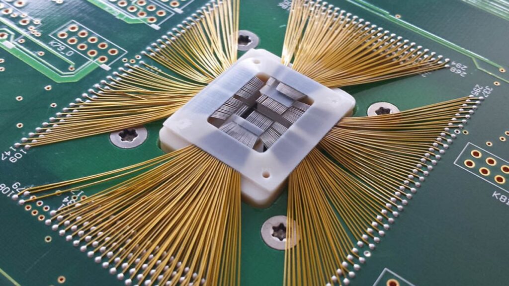
Probe Card Solutions
Fine-pitch vertical and cantilever probe architectures engineered for high-throughput wafer testing.
Precision Interconnects
High-density PCBA, flexible circuits, and multi-thickness Aluminum stiffeners for Preamp applications.
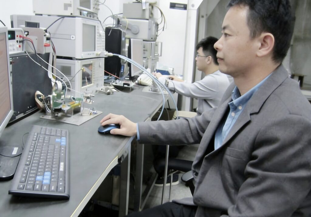
Calibration & Yield
Agilent-based measurement, register-level parameter write-back, and 100% serialized traceability.
Technical Capability Highlights
20 μm
6,000+
≤ 0.13%
0201
Quality Verification & Compliance
Certified Manufacturing Hub
Audited facility management at our Dongguan technical center. Scope: High-precision electronic assembly & test interface fabrication.
Calibration Excellence
Measurement equipment is calibrated against recognized reference standards with documented traceability to national physical references.
Japan, China & SE Asia Support
Strategic liaison offices serving global Tier-1 semiconductor supply chains from Hong Kong, Japan and Dongguan.
Engineering, Calibration & Assembly — All In House.
By maintaining full in-house control of the technical cycle—from multi-thickness stiffener lamination to software-based coefficient calculation—we ensure the precision required for high-pin-count semiconductor interfaces.
Discuss Your Probe Card or Precision Interconnect Project
Submit your specifications for a technical feasibility review within 24 business hours.